After borrowing the “Dragon Book” from the library, I was interested in trying to write my own compiler. Without ever having looked at VHDL or Verilog, I thought about creating a language to “program” simple digital circuits.
Initially written in C, it is now a Rust application that parses and compiles source code in this hardware description language which I developed myself. It produces files that can be read by my LogicSimulator project, a web-based simulator for digital circuits.
I have written an extensive README containing a lot more details and instructions on how to use the compiler which is available on GitLab together with the source code: gitlab.com/maxkl2/hdl-compiler.
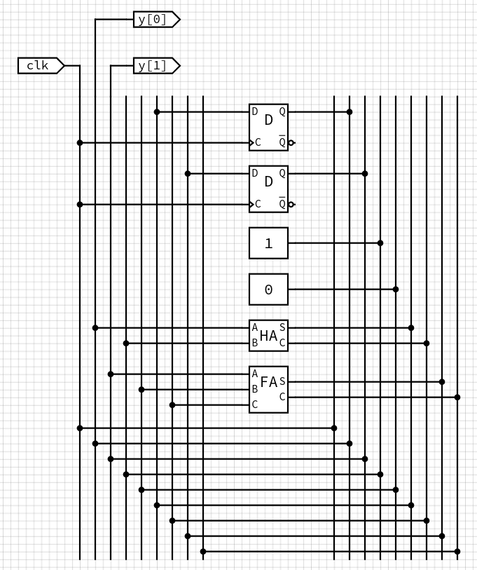
This is how a simple 2-bit counter would be implemented:
sequential block Counter {
    clock rising_edge clk;
    out[2] y;

    y = y + 1#2;
}

block main {
    in clk;
    out[2] y;

    block Counter c;
    c.clk = clk;
    y = c.y;
}
I did not implement any sophisticated graph drawing algorithm, so the circuits are not clearly layed out or aesthetically pleasing. The circuit generated from the code above looks like this:
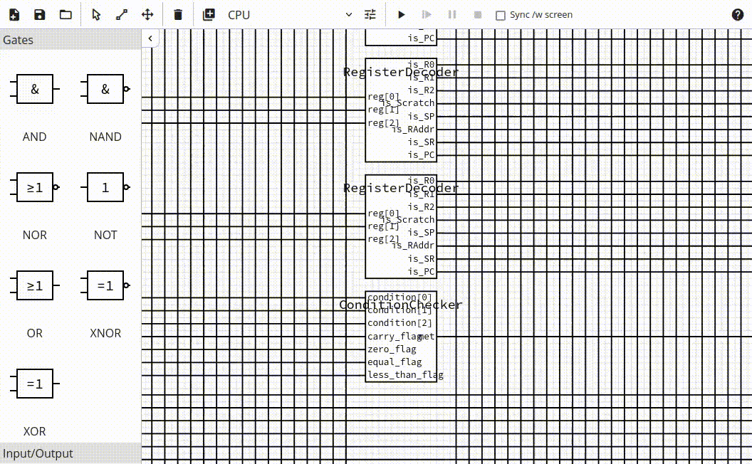
Example: 16-bit RISC CPU
To ensure the compiler’s correct functionality and to test its limits (especially regarding optimizations) I have written a 16-bit RISC core in this hardware description language: gitlab.com/maxkl2/hdl-cpu. The programs it executes can either be written by hand or created using a simple assembler that I created for this purpose. This assembler, also written in Rust, can be found in the same repository as the core’s HDL code.
This is a part of the circuit as generated by the compiler (yes, it’s ugly):
Here you can see a counter program which also reacts to user input:
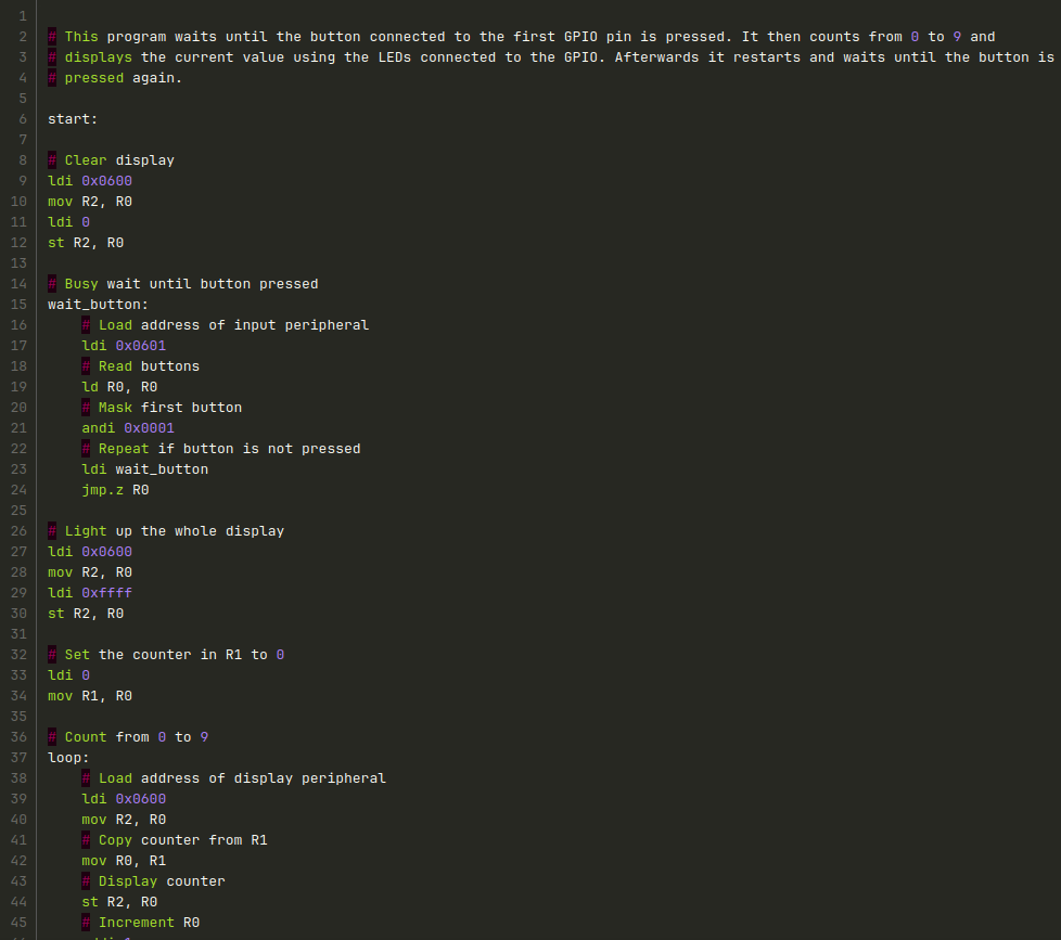
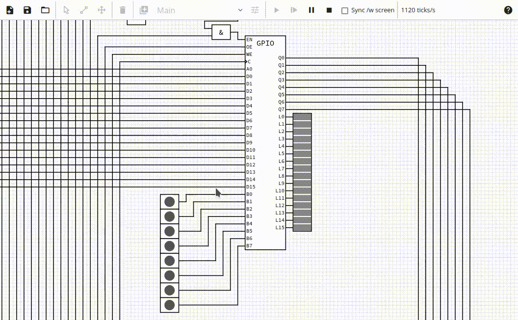
The CPU is capable of executing programs with subroutines, stack memory and memory-mapped peripherals. This is an excerpt of the README file, detailing the instruction set of the CPU:
Instruction set
The CPU implements a load/store architecture, inspired by existing RISC architectures such as MIPS and Arm.
There are eight 16-bit registers:
| Index | Register | Description |
|---|---|---|
| 0 | R0 | General purpose register 0. Target and source of instructions with immediate values. |
| 1 | R1 | General purpose register 1. |
| 2 | R2 | General purpose register 2. |
| 3 | Scratch | General purpose register which does not need to be preserved by subroutines. |
| 4 | SP | Stack Pointer. |
| 5 | RAddr | Return Address. Target register of the jal (“Jump And Link”) instruction. |
| 6 | SR | Status Register. Layout: 15-4: x, 3: LT (“Less Than”), 2: EQ (“EQuals”), 1: Z (“Zero”), 0: C (“Carry”) |
| 7 | PC | Program Counter. |
The bits 0-3 of the status register are set by the arithmetic and bitwise instructions as detailed below.
There are currently 22 (out of the possible 32) instructions. Every instruction executes in a single cycle.
| Instr. | Operation | Upd. flags | Opcode [15:11] | 10 | 9 | 8 | 7 | 6 | 5 | 4 | 3 | 2 | 1 | 0 |
|---|---|---|---|---|---|---|---|---|---|---|---|---|---|---|
| mov Rt, Rs | Rt = Rs | 0x00 | s | s | s | t | t | t | ||||||
| ld Rt, @Rs | Rt = @Rs | 0x01 | s | s | s | t | t | t | ||||||
| ldi imm | R0 = imm | 0x11 | i | i | i | i | i | i | i | i | i | i | i | |
| st @Rt, Rs | @Rt = Rs | 0x02 | s | s | s | t | t | t | ||||||
| and Rt, Ra, Rb | Rt = Ra & Rb | Z | 0x03 | b | b | b | a | a | a | t | t | t | ||
| andi imm | R0 = R0 & imm | Z | 0x13 | i | i | i | i | i | i | i | i | i | i | i |
| or Rt, Ra, Rb | Rt = Ra | Rb | Z | 0x04 | b | b | b | a | a | a | t | t | t | ||
| ori imm | R0 = R0 | imm | Z | 0x14 | i | i | i | i | i | i | i | i | i | i | i |
| xor Rt, Ra, Rb | Rt = Ra ^ Rb | Z | 0x05 | b | b | b | a | a | a | t | t | t | ||
| xori imm | R0 = R0 ^ imm | Z | 0x15 | i | i | i | i | i | i | i | i | i | i | i |
| not Rt, Rs | Rt = ~Rs | Z | 0x06 | s | s | s | t | t | t | |||||
| add Rt, Ra, Rb | Rt = Ra + Rb | Z, C | 0x07 | b | b | b | a | a | a | t | t | t | ||
| addi imm | R0 = R0 + imm | Z, C | 0x17 | i | i | i | i | i | i | i | i | i | i | i |
| sub Rt, Ra, Rb | Rt = Ra - Rb | Z, C | 0x08 | b | b | b | a | a | a | t | t | t | ||
| subi imm | R0 = R0 - imm | Z, C | 0x18 | i | i | i | i | i | i | i | i | i | i | i |
| sl Rt, Ra, Rb | Rt = Ra << Rb | Z | 0x09 | b | b | b | a | a | a | t | t | t | ||
| sli imm | R0 = R0 << imm | Z | 0x19 | i | i | i | i | |||||||
| sr Rt, Ra, Rb | Rt = Ra >> Rb | Z | 0x0A | b | b | b | a | a | a | t | t | t | ||
| sri imm | R0 = R0 >> imm | Z | 0x1A | i | i | i | i | |||||||
| cmp Ra, Rb | Ra - Rb | LT, EQ | 0x0B | b | b | b | a | a | a | |||||
| cmpi imm | R0 - imm | LT, EQ | 0x1B | i | i | i | i | i | i | i | i | i | i | i |
| jmp.cond Rs | if cond: PC = Rs | 0x0C | 0 | s | s | s | c | c | c | |||||
| jal.cond Rs | if cond: RAddr = PC; PC = Rs | 0x0C | 1 | s | s | s | c | c | c |
The ld and st instructions access the memory, where the “@” sign indicates that a register is interpreted as an absolute address. The letters in the rightmost columns denote the operands as follows:
| Letter | Description |
|---|---|
| t | Target register |
| s, a, b | Source registers |
| i | Immediate value |
| c | Condition code |
The jmp/jal instruction can be executed conditionally, with the following possible conditions:
| Code | Mnemonic | Behaviour | Description |
|---|---|---|---|
| 0 | <none> | Always executed | |
| 1 | z | SR.Z == 1 | Zero |
| 2 | eq | SR.EQ == 1 | Equal |
| 3 | ne | SR.EQ == 0 | Not equal |
| 4 | lt | SR.LT == 1 | Less than |
| 5 | le | SR.LT == 1 || SR.EQ == 1 | Less than or equal |
| 6 | gt | SR.LT == 0 && SR.EQ == 0 | Greater than |
| 7 | ge | SR.LT == 0 | Greater than or equal |